


ADE7753
–6–
REV. PrC 01/02
PRELIMINARY TECHNICAL DATA
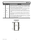
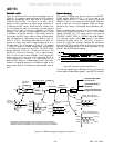
PIN FUNCTION DESCRIPTIONPIN FUNCTION DESCRIPTION
PIN FUNCTION DESCRIPTIONPIN FUNCTION DESCRIPTION
PIN FUNCTION DESCRIPTION
Pin No.Pin No.
Pin No.Pin No.
Pin No.
MNEMONICMNEMONIC
MNEMONICMNEMONIC
MNEMONIC
DESCRIPTIONDESCRIPTION
DESCRIPTIONDESCRIPTION
DESCRIPTION
1
RESET Reset pin for the ADE7753. A logic low on this pin will hold the ADCs and digital
circuitry (including the Serial Interface) in a reset condition.
2DV
DD
Digital power supply. This pin provides the supply voltage for the digital circuitry in
the ADE7753. The supply voltage should be maintained at 5V ± 5% for specified op-
eration. This pin should be decoupled to DGND with a 10µF capacitor in parallel with
a ceramic 100nF capacitor.
3AV
DD
Analog power supply. This pin provides the supply voltage for the analog circuitry in
the ADE7753. The supply should be maintained at 5V ± 5% for specified operation.
Every effort should be made to minimize power supply ripple and noise at this pin by
the use of proper decoupling. The typical performance graphs in this data sheet show
the power supply rejection performance. This pin should be decoupled to AGND with a
10µF capacitor in parallel with a ceramic 100nF capacitor.
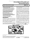
4,5 V1P, V1N Analog inputs for Channel 1. This channel is intended for use with the di/dt current
transducer such as Rogowski coil or other current sensor such as shunt or current trans-
former (CT). These inputs are fully differential voltage inputs with maximum
differential input signal levels of ±0.5V, ±0.25V and ±0.125V, depending on the full
scale selection - See Analog Inputs. Channel 1 also has a PGA with gain selections of 1,
2, 4, 8 or 16. The maximum signal level at these pins with respect to AGND is ±0.5V.
Both inputs have internal ESD protection circuitry and in addition an overvoltage of
±6V can be sustained on these inputs without risk of permanent damage.
6,7 V2N, V2P Analog inputs for Channel 2. This channel is intended for use with the voltage trans-
ducer. These inputs are fully differential voltage inputs with a maximum differential
signal level of ±0.5V. Channel 2 also has a PGA with gain selections of 1, 2, 4, 8 or
16. The maximum signal level at these pins with respect to AGND is ±0.5V. Both
inputs have internal ESD protection circuitry, and an overvoltage of ±6V can be sus-
tained on these inputs without risk of permanent damage.
8 AGND This pin provides the ground reference for the analog circuitry in the ADE7753, i.e.
ADCs and reference. This pin should be tied to the analog ground plane or the quietest
ground reference in the system. This quiet ground reference should be used for all ana-
log circuitry, e.g. anti-aliasing filters, current and voltage transducers etc. In order to
keep ground noise around the ADE7753 to a minimum, the quiet ground plane should
only connected to the digital ground plane at one point. It is acceptable to place the
entire device on the analog ground plane - see Applications Information.
9 REF
IN/OUT
This pin provides access to the on-chip voltage reference. The on-chip reference has a
nominal value of 2.4V ± 8% and a typical temperature coefficient of 20ppm/°C. An
external reference source may also be connected at this pin. In either case this pin
should be decoupled to AGND with a 1µF ceramic capacitor.
10 DGND This provides the ground reference for the digital circuitry in the ADE7753, i.e. multi-
plier, filters and digital-to-frequency converter. Because the digital return currents in
the ADE7753 are small, it is acceptable to connect this pin to the analog ground plane
of the system - see Applications Information. However, high bus capacitance on the DOUT
pin may result in noisy digital current which could affect performance.
11 C F Calibration Frequency logic output. The CF logic output gives Active Power informa-
tion. This output is intended to be used for operational and calibration purposes. The
full-scale output frequency can be adjusted by writing to the CFDEN and CFNUM
Register—see Energy To Frequency Conversion.
12 ZX Voltage waveform (Channel 2) zero crossing output. This output toggles logic high and
low at the zero crossing of the differential signal on Channel 2—see Zero Crossing Detection.
13
SAG This open drain logic output goes active low when either no zero crossings are detected
or a low voltage threshold (Channel 2) is crossed for a specified duration. See Line Volt-
age Sag Detection.
14
IRQ Interrupt Request Output. This is an active low open drain logic output. Maskable
interrupts include: Active Energy Register roll-over, Active Energy Register at half
level, and arrivals of new waveform samples. See ADE7753 Interrupts.