


ADE7753
–11–
REV. PrC 01/02
PRELIMINARY TECHNICAL DATA
ZERO CROSSING DETECTIONZERO CROSSING DETECTION
ZERO CROSSING DETECTIONZERO CROSSING DETECTION
ZERO CROSSING DETECTION
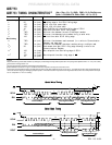
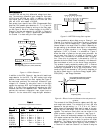
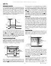
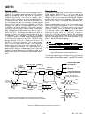
The ADE7753 has a zero crossing detection circuit on
Channel 2. This zero crossing is used to produce an external
zero cross signal (ZX) and it is also used in the calibration
mode - see Energy Calibration. The zero crossing signal is also
used to initiate a temperature measurement on the ADE7753
- see Temperature Measurement.
Figure 10 shows how the zero cross signal is generated from
the output of LPF1.
V2P
V2N
ADC 2
PGA2
1
x1, x2, x4,
x8, x16
REFERENCE
GAIN[7:5]
V2
TO
MULTIPLIER
-63% to + 63% FS
LPF1
f
-3dB
= 140Hz
ZERO
CROSS
ZX
V2
LPF1
ZX
23.2 Њ @ 60Hz
0.92
1.0
Figure 10– Zero cross detection on Channel 2
The ZX signal will go logic high on a positive going zero
crossing and logic low on a negative going zero crossing on
Channel 2. The zero crossing signal ZX is generated from the
output of LPF1. LPF1 has a single pole at 156Hz (at CLKIN
= 3.579545MHz). As a result there will be a phase lag
between the analog input signal V2 and the output of LPF1.
The phase response of this filter is shown in the Channel 2
Sampling section of this data sheet. The phase lag response of
LPF1 results in a time delay of approximately 0.97ms (@
60Hz) between the zero crossing on the analog inputs of
Channel 2 and the rising or falling edge of ZX.
The zero-crossing detection also drives one flag bit in the
interrupt status register. An active low in the IRQ output will
also appear if the corresponding bit in the Interrupt Enable
register is set to logic one.
The flag in the Interrupt status register as well as the IRQ
output are reset to their default value when the Interrupt
Status register with reset (RSTSTATUS) is read.
Zero crossing Time outZero crossing Time out
Zero crossing Time outZero crossing Time out
Zero crossing Time out
The zero crossing detection also has an associated time-out
register ZXTOUT. This unsigned, 12-bit register is
decremented (1 LSB) every 128/CLKIN seconds. The reg-
ister is reset to its user programmed full scale value every time
a zero crossing on Channel 2 is detected. The default power
on value in this register is FFFh. If the register decrements
to zero before a zero crossing is detected and the DISSAG bit
in the Mode register is logic zero, the 5)/ pin will go active
low. The absence of a zero crossing is also indicated on the
143 pin if the SAG enable bit in the Interrupt Enable register
is set to logic one. Irrespective of the enable bit setting, the
SAG flag in the Interrupt Status register is always set when
the ZXTOUT register is decremented to zero - see ADE7753
Interrupts.
The Zerocross Time-out register can be written/read by the
user and has an address of 1Dh - see Serial Interface section. The
resolution of the register is 128/CLKIN seconds per LSB.
Thus the maximum delay for an interrupt is 0.15 second
(128/CLKIN × 2
12
).
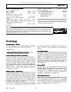
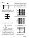
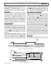
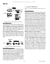
Figure 11 shows the mechanism of the zero crossing time out
detection when the line voltage stays at a fixed DC level for
more than CLKIN/128 x ZXTOUT seconds.
Channel 2
ZXTO
detection bit
ZXTOUT
16-bit internal
register value
Figure 11 - Zero crossing Time out detection
PERIOD MEASUREMENTPERIOD MEASUREMENT
PERIOD MEASUREMENTPERIOD MEASUREMENT
PERIOD MEASUREMENT
The ADE7753 provides also the period measurement of the
line. The period register is an unsigned 15-bit register and is
updated every period of the selected phase.
The resolution of this register is 2.2ms/LSB when
CLKIN=3.579545MHz, which represents 0.013% when the
line frequency is 60Hz. When the line frequency is 60Hz, the
value of the Period register is approximately 7576d. The
length of the register enables the measurement of line
frequencies as low as 13.9Hz.
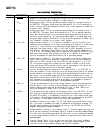
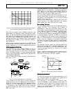
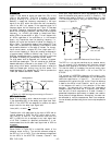
40 45 50 55 60 65 70
-90.02
-90.015
-90.01
-90.005
-90
-89.995
-89.99
-89.985
FREQUENCY-Hz
PHASE-DEGREES
Figure 9– Combined phase response of the digital integra-
tor and phase compensator (40Hz to 70Hz)
Note that the integrator has a -20dB/dec attenuation and
approximately -90° phase shift. When combined with a di/dt
sensor, the resulting magnitude and phase response should be
a flat gain over the frequency band of interest. However, the
di/dt sensor has a 20dB/dec gain associated with it, and
generates significant high frequency noise, a more effective
anti-aliasing filter is needed to avoid noise due to aliasing—
see Antialias Filter.
When the digital integrator is switched off, the ADE7753 can
be used directly with a conventional current sensor such as
current transformer (CT) or a low resistance current shunt.