


ADE7753
–29–
REV. PrC 01/02
PRELIMINARY TECHNICAL DATA
ADE7753 SERIAL INTERFACEADE7753 SERIAL INTERFACE
ADE7753 SERIAL INTERFACEADE7753 SERIAL INTERFACE
ADE7753 SERIAL INTERFACE
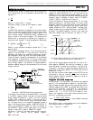
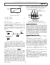
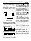
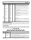
All ADE7753 functionality is accessible via several on-chip
registers – see Figure 49. The contents of these registers can
be updated or read using the on-chip serial interface. After
power-on or toggling the
RESET pin low or a falling edge
on
CS, the ADE7753 is placed in communications mode. In
communications mode the ADE7753 expects a write to its
Communications register. The data written to the communi-
cations register determines whether the next data transfer
operation will be read or a write and also which register is
accessed. Therefore all data transfer operations with the
ADE7753, whether a read or a write, must begin with a write
to the Communications register.
COMMUNICATIONS REGISTER
REGISTER # 1
REGISTER # 2
REGISTER # 3
REGISTER # n-1
REGISTER # n
IN
OUT
REGISTER ADDRESS
DECODE
DIN
DOUT
IN
OUT
IN
OUT
IN
OUT
IN
OUT
Figure 49– Addressing ADE7753 Registers via the
Communications Register
The Communications register is an eight bit wide register.
The MSB determines whether the next data transfer opera-
tion is a read or a write. The 5 LSBs contain the address of
the register to be accessed. See ADE7753 Communications Register
for a more detailed description.
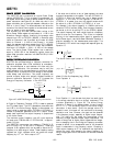
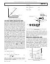
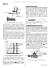
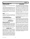
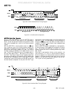
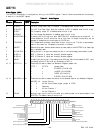
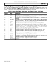
Figure 50 and 51 show the data transfer sequences for a read
and write operation respectively.
On completion of a data transfer (read or write) the ADE7753
once again enters communications mode.
COMMUNICATIONS REGISTER WRITE
CS
DIN
DOUT
SCLK
0 00
ADDRESS
MULTIBYTE READ DATA
Figure 50– Reading data from the ADE7753 via the serial
interface
COMMUNICATIONS REGISTER WRITE
CS
DIN
SCLK
1 00
ADDRESS
MULTIBYTE WRITE DATA
Figure 51– Writing data to the ADE7753 via the serial inter-
face
A data transfer is complete when the LSB of the ADE7753
register being addressed (for a write or a read) is transferred
to or from the ADE7753.
The Serial Interface of the ADE7753 is made up of four
signals SCLK, DIN, DOUT and
CS. The serial clock for a
data transfer is applied at the SCLK logic input. This logic
input has a schmitt-trigger input structure, which allows slow
rising (and falling) clock edges to be used. All data transfer
operations are synchronized to the serial clock. Data is
shifted into the ADE7753 at the DIN logic input on the
falling edge of SCLK. Data is shifted out of the ADE7753 at
the DOUT logic output on a rising edge of SCLK. The
CS
logic input is the chip select input. This input is used when
multiple devices share the serial bus. A falling edge on
CS
also resets the serial interface and places the ADE7753 in
communications mode. The CS input should be driven low
for the entire data transfer operation. Bringing
CS high
during a data transfer operation will abort the transfer and
place the serial bus in a high impedance state. The CS logic
input may be tied low if the ADE7753 is the only device on
the serial bus. However with
CS tied low, all initiated data
transfer operations must be fully completed, i.e., the LSB of
each register must be transferred as there is no other way of
bringing the ADE7753 back into communications mode
without resetting the entire device, i.e., using
RESET.
ADE7753 Serial Write OperationADE7753 Serial Write Operation
ADE7753 Serial Write OperationADE7753 Serial Write Operation
ADE7753 Serial Write Operation
The serial write sequence takes place as follows. With the
ADE7753 in communications mode (i.e. the
CS input logic
low), a write to the communications register first takes place.
The MSB of this byte transfer is a 1, indicating that the data
transfer operation is a write. The LSBs of this byte contain
the address of the register to be written to. The ADE7753
starts shifting in the register data on the next falling edge of
SCLK. All remaining bits of register data are shifted in on the
falling edge of subsequent SCLK pulses – see Figure 51.
As explained earlier the data write is initiated by a write to the
communications register followed by the data. During a data
write operation to the ADE7753, data is transferred to all on-
chip registers one byte at a time. After a byte is transferred
into the serial port, there is a finite time before it is transferred
to one of the ADE7753 on-chip registers. Although another
byte transfer to the serial port can start while the previous byte
is being transferred to an on-chip register, this second byte
transfer should not finish until at least 4µs after the end of the
previous byte transfer. This functionality is expressed in the
timing specification t
6
- see Figure 51. If a write operation is
aborted during a byte transfer (
CS brought high), then that
byte will not be written to the destination register.
Destination registers may be up to 3 bytes wide – see ADE7753
Register Descriptions. Hence the first byte shifted into the serial
port at DIN is transferred to the MSB (Most significant Byte)
of the destination register. If the addressed register is 12 bits
wide, for example, a two-byte data transfer must take place.
The data is always assumed to be right justified, therefore in
this case, the four MSBs of the first byte would be ignored and
the 4 LSBs of the first byte written to the ADE7753 would be
the 4MSBs of the 12-bit word. Figure 52 illustrates this
example.