


ADE7753
–12–
REV. PrC 01/02
PRELIMINARY TECHNICAL DATA
POWER SUPPLY MONITORPOWER SUPPLY MONITOR
POWER SUPPLY MONITORPOWER SUPPLY MONITOR
POWER SUPPLY MONITOR
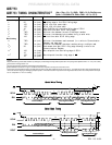
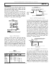
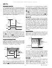
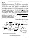
The ADE7753 also contains an on-chip power supply moni-
tor. The Analog Supply (AV
DD
) is continuously monitored
by the ADE7753. If the supply is less than 4V ± 5% then the
ADE7753 will go into an inactive state, i.e. no energy will be
accumulated when the supply voltage is below 4V. This is
useful to ensure correct device operation at power up and
during power down. The power supply monitor has built-in
hysteresis and filtering. This gives a high degree of immunity
to false triggering due to noisy supplies.
Time
AV
DD
0V
4V
5V
ADE7753
Power-on
Reset
Inactive
Active
Inactive
SAG
Figure 12 - On-Chip power supply monitor
As can be seen from Figure 12 the trigger level is nominally
set at 4V. The tolerance on this trigger level is about ±5%.
The
SAG pin can also be used as a power supply monitor
input to the MCU. The
SAG pin will go logic low when the
ADE7753 is reset. The power supply and decoupling for the
part should be such that the ripple at AV
DD
does not exceed
5V±5% as specified for normal operation.
LINE VOLTAGE SAG DETECTIONLINE VOLTAGE SAG DETECTION
LINE VOLTAGE SAG DETECTIONLINE VOLTAGE SAG DETECTION
LINE VOLTAGE SAG DETECTION
In addition to the detection of the loss of the line voltage
signal (zero crossing), the ADE7753 can also be pro-
grammed to detect when the absolute value of the line voltage
drops below a certain peak value, for a number of half cycles.
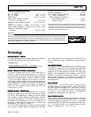
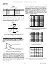
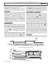
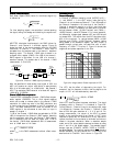
This condition is illustrated in Figure 13 below.
SAGCYC[7:0] = 06H
6 half cycles
SAGLVL[7:0]
Full Scale
Channel 2
SAG
SAG reset high
when Channel 2
exceeds SAGLVL[7:0]
Figure 13– ADE7753 Sag detection
Figure 13 shows the line voltage fall below a threshold which
is set in the Sag Level register (SAGLVL[7:0]) for nine half
cycles. Since the Sag Cycle register (SAGCYC[7:0]) con-
tains 06h the
SAG pin will go active low at the end of the sixth
half cycle for which the line voltage falls below the threshold,
if the DISSAG bit in the Mode register is logic zero. As is
the case when zero-crossings are no longer detected, the sag
event is also recorded by setting the SAG flag in the Interrupt
Status register. If the SAG enable bit is set to logic one, the
IRQ logic output will go active low - see ADE7753 Interrupts.
The
SAG pin will go logic high again when the absolute value
of the signal on Channel 2 exceeds the sag level set in the Sag
Level register. This is shown in Figure 13 when the
SAG pin
goes high during the tenth half cycle from the time when the
signal on Channel 2 first dropped below the threshold level.
Sag Level SetSag Level Set
Sag Level SetSag Level Set
Sag Level Set
The contents of the Sag Level register (1 byte) are compared
to the absolute value of the most significant byte output from
LPF1, after it is shifted left by one bit. Thus for example the
nominal maximum code from LPF1 with a full scale signal
on Channel 2 is 1C396h or (0001, 1100, 0011, 1001,
0110b)—see Channel 2 sampling. Shifting one bit left will give
0011,1000,0111,0010,1100b or 3872Ch. Therefore writing
38h to the Sag Level register will put the sag detection level
at full scale. Writing 00h will put the sag detection level at
zero. The Sag Level register is compared to the most
significant byte of a waveform sample after the shift left and
detection is made when the contents of the sag level register
are greater.
PEAK DETECTIONPEAK DETECTION
PEAK DETECTIONPEAK DETECTION
PEAK DETECTION
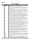
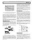
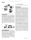
The ADE7753 can also be programmed to detect when the
absolute value of the voltage or the current channel of one
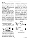
phase exceeds a certain peak value. Figure 14 illustrates the
behavior of the peak detection for the voltage channel.
VPKLVL[7:0]
V
2
PKV Interrupt Flag
(Bit C of STATUS register)
PKV reset low
when RSTSTATUS register
is read
Read RSTSTATUS register
Figure 14 - ADE7753 Peak detection
Both channel 1 and channel 2 can be monitored at the same
time. Figure 14 shows a line voltage exceeding a threshold
which is set in the Voltage peak register (VPKLVL[7:0]).
The Voltage Peak event is recorded by setting the PKV flag
in the Interrupt Status register. If the PKV enable bit is set to
logic one in the Interrupt Mask register, the
IRQ logic output
will go active low - see ADE7753 Interrupts.
Peak Level SetPeak Level Set
Peak Level SetPeak Level Set
Peak Level Set
The contents of the VPKLVL and IPKLVL registers are
respectively compared to the absolute value of channel 1 and
channel 2, after they are multiplied by 2.
Thus, for example, the nominal maximum code from the
channel 1 ADC with a full scale signal is 1C396h —see
Channel 1 Sampling. Multiplying by 2 will give 3872Ch.