


ADE7753
–34–
REV. PrC 01/02
PRELIMINARY TECHNICAL DATA
Mode Register (09H)Mode Register (09H)
Mode Register (09H)Mode Register (09H)
Mode Register (09H)
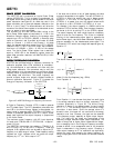
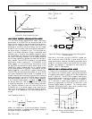
The ADE7753 functionality is configured by writing to the MODE register. Table VI below summarizes the functionality
of each bit in the MODE register .
Table VI : Mode RegisterTable VI : Mode Register
Table VI : Mode RegisterTable VI : Mode Register
Table VI : Mode Register
BitBit
BitBit
Bit
BitBit
BitBit
Bit
DefaultDefault
DefaultDefault
Default
LocationLocation
LocationLocation
Location
MnemonicMnemonic
MnemonicMnemonic
Mnemonic
ValueValue
ValueValue
Value
DescriptionDescription
DescriptionDescription
Description
0 DISHPF 0 The HPF (High Pass Filter) in Channel 1 is disabled when this bit is set.
1 DISLPF2 0 The LPF (Low Pass Filter) after the multiplier (LPF2) is disabled when this bit is set.
2 DISCF 1 The Frequency output CF is disabled when this bit is set
3 DISSAG 1 The line voltage Sag detection is disabled when this bit is set
4 ASUSPEND 0 By setting this bit to logic one, both ADE7753's A/D converters can be turned off. In
normal operation, this bit should be left at logic zero. All digital functionality can be
stopped by suspending the clock signal at CLKIN pin.
5 TEMPSEL 0 The Temperature conversion starts when this bit is set to one. This bit is automatically
reset to zero when the Temperature conversion is finished.
6 SWRST 0 Software chip reset. A data transfer should not take place to the ADE7753 for at least 18µs
after a software reset.
7 CYCMODE 0 Setting this bit to a logic one places the chip in line cycle energy accumulation mode.
8 DISCH1 0 ADC 1 (Channel 1) inputs are internally shorted together.
9 DISCH2 0 ADC 2 (Channel 2) inputs are internally shorted together.
10 SWAP 0 By setting this bit to logic 1 the analog inputs V2P and V2N are connected to ADC 1 and
the analog inputs V1P and V1N are connected to ADC 2.
12, 11 DTRT1,0 00 These bits are used to select the Waveform Register update rate
DTRT 1 DTRT0 Update Rate
0 0 27.9kSPS (CLKIN/128)
0 1 14kSPS (CLKIN/256)
1 0 7kSPS (CLKIN/512)
1 1 3.5kSPS (CLKIN/1024)
14, 13 WAVSEL1,0 00 These bits are used to select the source of the sampled data for the Waveform Register
WAVSEL1,0 Length Source
0 0 24 bits Active Power signal (output of LPF2)
0 1 Reserved
1 0 24 bits Channel 1
1 1 24 bits Channel 2
15 POAM 0 Writing a logic one to this bit will allow only positive power to be accumulated in the
ADE7753. The default value of this bit is 0.
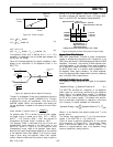
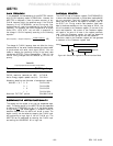
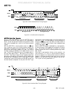
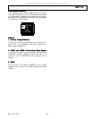
MODE REGISTER*
ADDR: 09H
01234
5
67
00110000
POAM
(Positive Only Accumulation)
WAVSEL
(Wave form selection for sample mode)
00 = LPF2
01= Reserved
10 = CH1
11 = CH2
DISHPF
(Disable HPF in Channel 1)
DISLPF2
DISCF
(Disable Frequency output CF)
DISSAG
(Disable SAG output)
*Register contents show power on defaults
(Suspend CH1&CH2 ADC’s)
89101112
13
1415
00000000
DTRT
(Waveform samples output data rate)
00 = 27.9kSPS (CLKIN/128)
01 = 14.4 kSPS (CLKIN/256)
10 = 7.2 kSPS (CLKIN/512)
11 = 3.6 kSPS (CLKIN/1024)
SWAP
(Swap CH1 & CH2 ADCs)
DISCH2
(Short the analog inputs on Channel 2)
DISCH1
(Short the analog inputs on Channel 1)
SWRST
(Software chip reset)
CYCMODE
(Line Cycle Energy Accumulation Mode)
(Disable LPF2 after multiplier)
STEMP
ASUSPEND
(Start temperature sensing)