


ADE7753
–32–
REV. PrC 01/02
PRELIMINARY TECHNICAL DATA
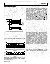
AddressAddress
AddressAddress
Address
NameName
NameName
Name
R/WR/W
R/WR/W
R/W
# of Bits# of Bits
# of Bits# of Bits
# of Bits
DefaultDefault
DefaultDefault
Default
DescriptionDescription
DescriptionDescription
Description
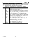
10h PHCAL R/W 6 bits 0h Phase Calibration register. The phase relationship between
Channel 1 and 2 can be adjusted by writing to this 6-bit register.
The valid content of this 2's compliment register is between 1Fh
to 20h, which a phase difference of -0.748° to +0.748° at 60Hz
in 0.0241° steps—see Phase Compensation.
11h APOS R/W 16 bits 0h Active Power Offset Correction. This 16-bit register allows small
offsets in the Active Power Calculation to be removed – see
Active Power Calculation.
12h WGAIN R/W 12 bits 0h Power Gain Adjust. This is a 12-bit register. The Active Power
calculation can be calibrated by writing to this register. The
calibration range is ±50% of the nominal full scale active power.
The resolution of the gain adjust is 0.0244% / LSB—see Channel
1 ADC Gain Adjust.
13h WDIV R/W 8 bits 0h Active Energy divider register. The internal active energy register
is divided by the value of this register before being stored in the
AENERGY register.
14h CFNUM R/W 12 bits 3Fh CF Frequency Divider Numerator register. The output frequency
on the CF pin is adjusted by writing to this 12-bit read/write
register – see Energy to Frequency Conversion.
15h CFDEN R/W 12 bits 3Fh CF Frequency Divider Denominator register. The output
frequency on the CF pin is adjusted by writing to this 12-bit
read/write register – see Energy to Frequency Conversion.
16h IRMS R 24 bits 0h Channel 1 RMS value (current channel).
17h VRMS R 24 bits 0h Channel 2 RMS value (voltage channel).
18h IRMSOS R/W 12 bits 0h Channel 1 RMS offset correction register
19h VRMSOS R/W 12 bits 0h Channel 2 RMS offset correction register
1Ah VAGAIN R/W 12 bits 0h Apparent Gain register. Apparent power calculation can be
calibrated by writing this register. The calibration range is 50%
of the nominal full scale real power. The resolution of the gain
adjust is 0.02444% / LSB.
1Bh VADIV R/W 8 bits 0h Apparent Energy divider register. The internal apparent energy
register is divided by the value of this register before being stored
in the VAENERGY register.
1Ch LINECYC R/W 16 bits FFFFh Line Cycle Energy Accumulation Mode Half-Cycle register.
This 16-bit register is used during line cycle energy
accumulation mode to set the number of half line cycles active
energy is accumulated-see Line Cycle Energy Accumulation Mode.
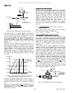
1Dh ZXTOUT R/W 12 bits FFFh Zero-cross Time Out. If no zero crossings are detected on
Channel 2 within a time period specified by this 12-bit register,
the interrupt request line (
IRQ) will be activated. The maximum
time-out period is 0.15 second - see Zero Crossing Detection.
1Eh SAGCYC R/W 8 bits FFh Sag line Cycle register. This 8-bit register specifies the number
of consecutive half line cycles the signal on Channel 2 must be
below SAGLVL before the
SAG output is activated - see Voltage
Sag Detection
1Fh SAGLVL R/W 8 bits 0h Sag Voltage Level. An 8-bit write to this register determines at
what peak signal level on Channel 2 the SAG pin will become
active. The signal must remain low for the number of cycles
specified in the SAGCYC register before the SAG pin is
activated—see Line Voltage Sag Detection.
20h IPKLVL R/W 8 bits FFh Channel 1 Peak Level threshold (current channel). This register
sets the level of the current peak detection. If the channel 1 input
exceeds this level, the PKI flag in the status register is set.