


ADE7753
–31–
REV. PrC 01/02
PRELIMINARY TECHNICAL DATA
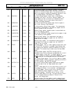
ADE7753 REGISTER LISTADE7753 REGISTER LIST
ADE7753 REGISTER LISTADE7753 REGISTER LIST
ADE7753 REGISTER LIST
AddressAddress
AddressAddress
Address
NameName
NameName
Name
R/WR/W
R/WR/W
R/W
# of Bits# of Bits
# of Bits# of Bits
# of Bits
DefaultDefault
DefaultDefault
Default
DescriptionDescription
DescriptionDescription
Description
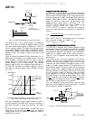
01h WAVEFORM R 24 bits 0h The Waveform register is a read-only register. This register
contains the sampled waveform data from either Channel 1,
Channel 2 or the Active Power signal. The data source and the
length of the waveform registers are selected by data bits 14 and
13 in the Mode Register - see Channel 1 & 2 Sampling.
02h AENERGY R 24 bits 0h The Active Energy register. Active Power is accumulated
(Integrated) over time in this 24-bit, read-only register. The
energy register can hold a minimum of 6 seconds of Active
Energy information with full scale analog inputs before it
overflows - see Energy Calculation.
03h RAENERGY R 24 bits 0h Same as the Active Energy register except that the register is
reset to zero following a read operation
04h LAENERGY R 24 bits 0h Line Accumulation Active Energy register. The instantaneous
active power is accumulated in this read-only register over the
LINCYC number of half line cycles.
05h VAENERGY R 24 bits 0h Apparent Energy register. Apparent power is accumulated over
time in this read-only register.
06h RVAENERGY R 24 bits 0h Same as the VAENERGY register except that the register is reset
to zero following a read operation.
07h LVAENERGY R 24 bits 0h Apparent Energy register. The instantaneous real power is
accumulated in this read-only register over the LINECYC
number of half line cycles
08h LVARENERGY R 24 bits 0h Reactive Energy register. The instantaneous reactive power is
accumulated in this read-only register over the LINECYC
number of half line cycles.
09h MODE R/W 16 bits 000Ch The Mode register. This is a 16-bit register through which most
of the ADE7753 functionality is accessed. Signal sample rates,
filter enabling and calibration modes are selected by writing to
this register. The contents may be read at any time—see Mode
Register.
0Ah IRQEN R/W 16 bits 0h Interrupt Enable register. ADE7753 interrupts may be
deactivated at any time by setting the corresponding bit in this 8-
bit Enable register to logic zero. The Status register will
continue to register an interrupt event even if disabled. However,
the
IRQ output will not be activated—see ADE7753 Interrupts.
0Bh STATUS R 16 bits 0h The Interrupt Status register. This is an 8-bit read-only register.
The Status Register contains information regarding the source of
ADE7753 interrupts - see ADE7753 Interrupts.
0Ch RSTSTATUS R 16 bits 0h Same as the Interrupt Status register except that the register
contents are reset to zero (all flags cleared) after a read
operation.
0Dh CH1OS R/W 8 bits 00h Channel 1 Offset Adjust. Bit 6 is not used. Writing to bits 0 to 5
allows offsets on Channel 1 to be removed – see Analog Inputs
and CH1OS Register. Writing a logic one to the MSB of this
register enables the digital integrator on Channel 1, a zero
disables the integrator. The default value of this bit is zero.
0Eh CH2OS R/W 8 bits 0h Channel 2 Offset Adjust. Bit 6 and 7 not used. Writing to bits 0
to 5 of this register allows any offsets on Channel 2 to be
removed - see Analog Inputs.
0Fh GAIN R/W 8 bits 0h PGA Gain Adjust. This 8-bit register is used to adjust the gain
selection for the PGA in Channel 1 and 2 - see Analog Inputs.