30
4173ES–USB–09/07
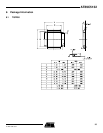
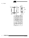
AT89C5132
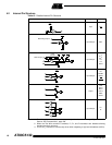
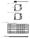
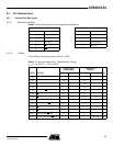
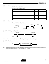
6.3.7 Analog to Digital Converter
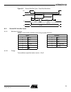
6.3.7.1 Definition of Symbols
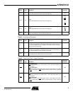
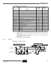
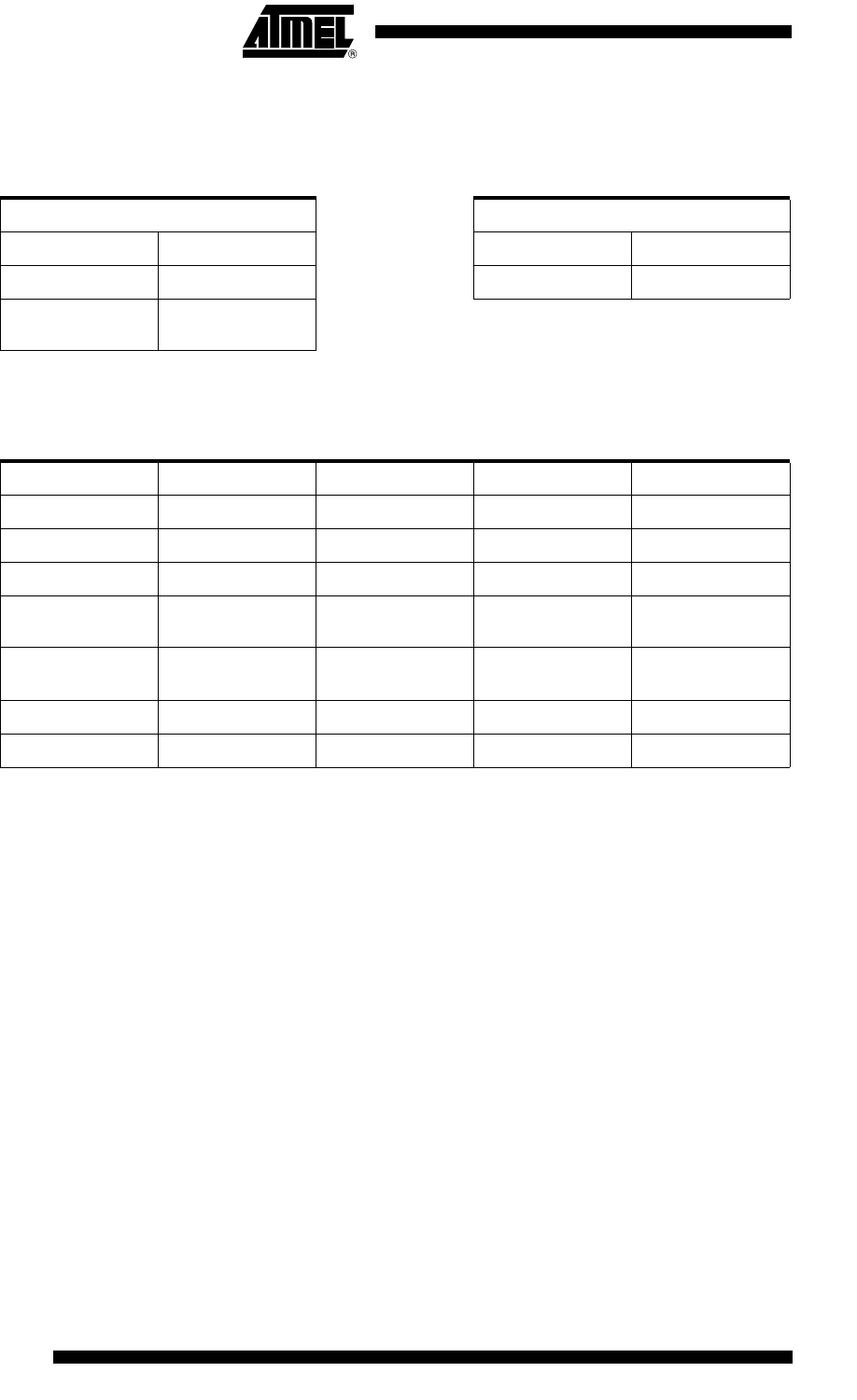
Table 18. Analog to Digital Converter Timing Symbol Definitions
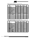
6.3.7.2 Characteristics
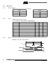
Table 18. Analog to Digital Converter AC Characteristics
V
DD
= 2.7 to 3.3 V, T
A
= -40 to +85°C
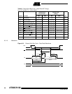
Notes: 1. AV
DD
= AV
REFP
= 3.0 V, AV
SS
= AV
REFN
= 0 V. ADC is monotonic with no missing code.
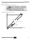
2. The differential non-linearity is the difference between the actual step width and the ideal step
width (see
Figure 6-20).
3. The integral non-linearity is the peak difference between the center of the actual step and the
ideal transfer curve after appropriate adjustment of gain and offset errors (see
Figure 6-20).
4. The offset error is the absolute difference between the straight line which fits the actual trans-
fer curve (after removing of gain error), and the straight line which fits the ideal transfer curve
(see
Figure 6-20).
5. The gain error is the relative difference in percent between the straight line which fits the actual
transfer curve (after removing of offset error), and the straight line which fits the ideal transfer
curve (see
Figure 6-20).
Signals Conditions
C Clock H High
E Enable (ADEN bit) L Low
S
Start Conversion
(ADSST bit)
Symbol Parameter Min Max Unit
T
CLCL
Clock Period 4 μs
T
EHSH
Start-up Time 4 μs
T
SHSL
Conversion Time 11·T
CLCL
μs
DLe
Differential non-
linearity error
(1)(2)
1LSB
ILe
Integral non-linearity
errorss
(1)(3)
2LSB
OSe Offset error
(1)(4)
4LSB
Ge Gain error
(1)(5)
4LSB