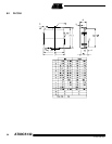
15
4173ES–USB–09/07
AT89C5132
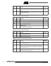
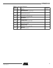
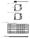
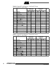
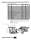
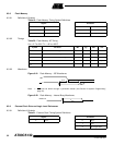
Notes: 1. Typical values are obtained using V
DD
= 3 V and T
A
= 25°C. They are not tested and there is no
guarantee on these values.
2. Flash retention is guaranteed with the same formula for V
DD
min down to 0V.
3. See Table 154 for typical consumption in player mode.
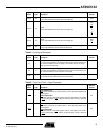
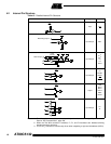
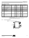
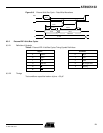
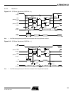
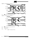
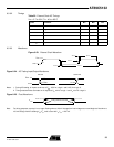
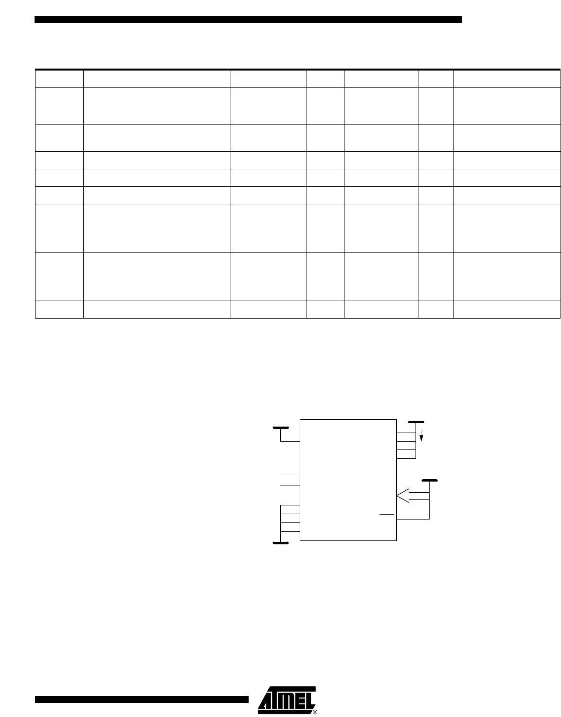
6.2.2 I
DD,
I
DL
and I
PD
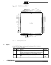
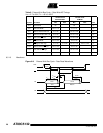
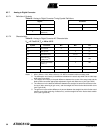
Test Conditions
Figure 6-1. I
DD
Test Condition, Active Mode
I
LI
Input Leakage Current (P0, ALE, MCMD,
MDAT, MCLK, SCLK, DCLK, DSEL,
DOUT)
10 μA 0.45< V
IN
< V
DD
I
TL
Logical 1 to 0 Transition Current
(P1, P2, P3, P4 and P5)
-650 μA Vin = 2.0 V
R
RST
Pull-Down Resistor 50 90 200 kΩ
C
IO
Pin Capacitance 10 pF T
A
= 25°C
V
RET
V
DD
Data Retention Limit 1.8 V
I
DD
Operating Current
(3)
X1 / X2 mode
6.5 / 10.5
8 / 13.5
9.5 / 17
mA
V
DD
< 3.3 V
12 MHz
16 MHz
20 MHz
I
DL
Idle Mode Current
(3)
X1 / X2 mode
5.3 / 8.1
6.4 / 10.3
7.5 / 13
mA
V
DD
< 3.3 V
12 MHz
16 MHz
20 MHz
I
PD
Power-Down Mode Current 20 500 μAV
RET
< V
DD
< 3.3 V
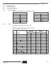
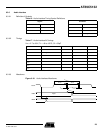
Table 1. Digital DC Characteristics
V
DD
= 2.7 to 3.3V , T
A
= -40 to +85°C
Symbol Parameter Min Typ
(1)
Max Units Test Conditions
RST
TST
P0
All other pins are unconnected
VDD
VDD
VDD
I
DD
VDD
PVDD
UVDD
AVDD
X2
Clock Signal
VSS
X1
(NC)
VSS
PVSS
UVSS
AVSS