27
4173ES–USB–09/07
AT89C5132
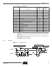
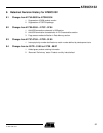
V
DD
= 2.7 to 3.3 V, T
A
= -40 to +85°C
Notes: 1. At 100 kbit/s. At other bit-rates this value is inversely proportional to the bit-rate of 100 kbit/s.
2. Determined by the external bus-line capacitance and the external bus-line pull-up resistor, this
must be < 1 μs.
3. Spikes on the SDA and SCL lines with a duration of less than 3·TCLCL will be filtered out. Maxi-
mum capacitance on bus-lines SDA and
SCL= 400 pF.
4. TCLCL= T
OSC
= one oscillator clock period.
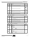
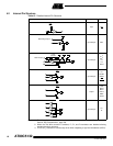
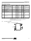
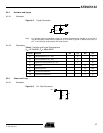
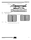
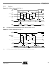
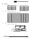
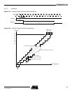
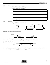
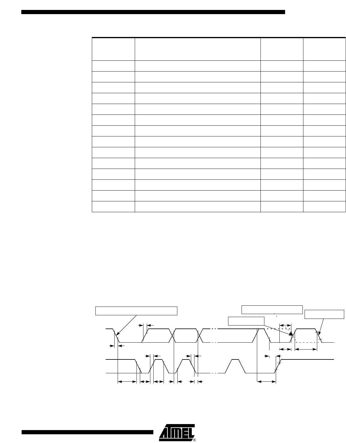
6.3.4.2 Waveforms
Figure 6-16. Two Wire Waveforms
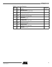
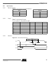
Symbol Parameter
INPUT
Min
Max
OUTPUT
Min
Max
T
HD; STA Start condition hold time 14·TCLCL
(4)
4.0 μs
(1)
TLOW SCL low time 16·TCLCL
(4)
4.7 μs
(1)
THIGH SCL high time 14·TCLCL
(4)
4.0 μs
(1)
TRC SCL rise time 1 μs-
(2)
TFC SCL fall time 0.3 μs0.3 μs
(3)
TSU; DAT1 Data set-up time 250 ns 20·TCLCL
(4)
- TRD
TSU; DAT2 SDA set-up time (before repeated START condition) 250 ns 1 μs
(1)
TSU; DAT3 SDA set-up time (before STOP condition) 250 ns 8·TCLCL
(4)
THD; DAT Data hold time 0 ns 8·TCLCL
(4)
- TFC
TSU; STA Repeated START set-up time 14·TCLCL
(4)
4.7 μs
(1)
TSU; STO STOP condition set-up time 14·TCLCL
(4)
4.0 μs
(1)
TBUF Bus free time 14·TCLCL
(4)
4.7 μs
(1)
TRD SDA rise time 1 μs -
(2)
TFD SDA fall time 0.3 μs0.3 μs
(3)
Tsu;DAT1
T
su
;STA
Tsu;DAT2
T
hd
;STA
T
high
T
low
SDA
(INPUT/OUTPUT)
0.3 V
DD
0.7 V
DD
T
buf
T
su
;STO
0.7
V
DD
0.3 V
DD
T
rd
T
fd
T
rc
T
fc
SCL
(INPUT/OUTPUT)
T
hd;
DAT
T
su;
DAT3
START or Repeated START condition
START condition
STOP condition
Repeated START condition