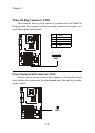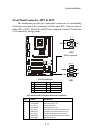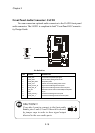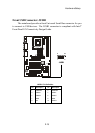
Chapter 3
3-12
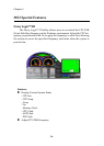
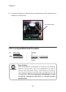
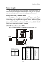
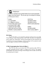
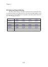
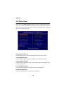
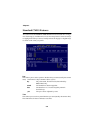
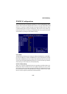
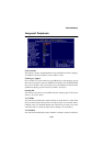
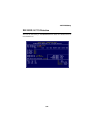
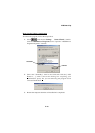
Advanced Chipset Features
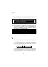
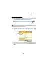
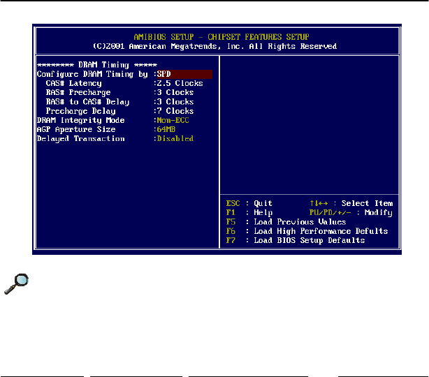
Configure DRAM Timing by
This setting determines whether DRAM timing is controlled by the SPD (Serial
Presence Detect) EEPROM on the DRAM module. Setting to SPD enables
CAS# Latency, RAS# Precharge, RAS# to CAS# Delay, and Precharge Delay
automatically to be determined by BIOS based on the configurations on the
SPD. Selecting Manual allows users to configure these fields manually.
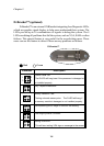
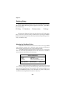
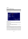
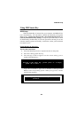
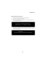
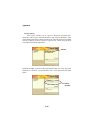
CAS# Latency
The field controls the CAS latency, which determines the timing delay before
SDRAM starts a read command after receiving it. Setting options: 2.5 Clocks,
2 Clocks. 2 Clocks increases system performance while 2.5 Clocks provides
more stable system performance.
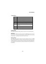
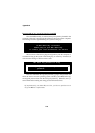
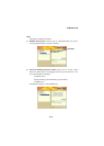
RAS# Precharge
This setting controls the number of cycles for Row Address Strobe (RAS) to
be allowed to precharge. If insufficient time is allowed for the RAS to accumu-
late its charge before DRAM refresh, refresh may be incomplete and DRAM
may fail to retain data. This item applies only when synchronous DRAM is
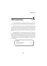
Note: Change these settings only if you are familiar with the chipset.